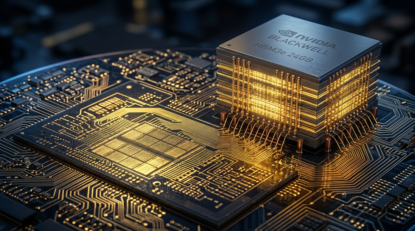
In the modern architecture of frontier artificial intelligence, the arithmetic logic unit has ceased to be the primary bottleneck. As transformer parameter counts scale into the multi-trillion regime, computational throughput is governed by the brutal physics of the Memory Wall—the widening divergence between compute capacity and memory bandwidth. The battle for silicon supremacy is won not in the transistor gates alone, but within the micro-bump pitch of silicon interposers and the communication topologies of distributed tensor parallel pipelines.
Key Architecture Insight
In large language model pretraining, operational intensity (FLOPs per byte of DRAM access) dictates whether an accelerator runs compute-bound or memory-bound. While matrix multiplication in feed-forward layers is compute-dense, attention mechanisms, normalization layers, and KV-cache autoregressive token generation are fundamentally bandwidth-starved.
1. The Physics of the Memory Moat: SK Hynix and HBM Evolution
High-Bandwidth Memory (HBM) achieves orders-of-magnitude higher throughput than standard GDDR or LPDDR by stacking DRAM dies vertically using Through-Silicon Vias (TSVs) over an ultra-wide 1024-bit memory interface per stack. With HBM3e achieving pin speeds of 9.6 Gbps to exceed 1.2 TB/s per stack, and upcoming HBM4 moving to a 2048-bit base interface on advanced foundry logic nodes, packaging thermodynamics have become the ultimate competitive moat.
| Generation | Stack Height | Bus Width | Max Pin Speed | Bandwidth per Stack | Packaging Technology |
|---|---|---|---|---|---|
| HBM3 | 8-Hi / 12-Hi | 1024-bit | 6.4 Gbps | 819 GB/s | Non-Conductive Film (NCF) |
| HBM3e | 12-Hi / 16-Hi | 1024-bit | 9.6 Gbps | 1.22 TB/s | Advanced MR-MUF (SK Hynix) |
| HBM4 | 16-Hi | 2048-bit | 10+ Gbps | 2.0+ TB/s | Direct Cu-Cu Hybrid Bonding |
Advanced MR-MUF vs. Traditional NCF
SK Hynix’s dominant market position in HBM3e stems from its pioneering adoption of Mass Reflow Molded Underfill (MR-MUF). Traditional Non-Conductive Film (NCF) stacks require laying a polymer film between every micro-bump layer and applying high-temperature thermo-compression bonding, which induces thermal warpage and uneven void formation across 12-high and 16-high stacks. MR-MUF places liquid epoxy molding material across all layers simultaneously after gang reflow, delivering 2.5x higher thermal conductivity and vastly superior mechanical yields.
For HBM4, the industry is transitioning to direct copper-to-copper (Cu-Cu) hybrid bonding (such as TSMC SoIC / Wafer-to-Wafer bonding), eliminating solder bumps altogether to shrink inter-die pitch below 1 micrometer and dramatically reduce parasitic capacitance.
2. TSMC CoWoS & The Reticle Limit Challenge
Integrating 8 to 16 HBM stacks alongside monolithic or multi-die compute chiplets requires heterogeneous packaging. TSMC’s CoWoS (Chip-on-Wafer-on-Substrate) has evolved through distinct technological branches:
- CoWoS-S: Utilizes a full monolithic passive silicon interposer with etched TSVs, delivering high interconnect density but constrained by optical lithography reticle limits (~858 mm²).
- CoWoS-L: Utilizes a local silicon interconnect (LSI) bridge embedded in an organic molding interposer with fine-pitch Redistribution Layers (RDL), enabling reticle sizes exceeding 3.3x to accommodate massive dual-die compute packages.
- CoWoS-R: Replaces the silicon interposer entirely with polymer-based organic thin-film layers for cost optimization in mid-tier accelerators.
“Silicon area is no longer defined by the reticle of a lithography scanner; it is defined by the thermal dissipation envelope of the package substrate and the high-frequency signal integrity of the interposer bridge.”
3. NVIDIA Blackwell B200 / GB200 NVLink-5 Architecture
The NVIDIA Blackwell architecture synthesizes these packaging advancements into an extreme compute topology. The B200 accelerator connects two full-reticle dies across a 10 TB/s ultra-high-density NV-HBI (High-Bandwidth Interconnect) link, presenting the pair to the CUDA runtime as a single coherent monolithic GPU with 192 GB of HBM3e delivering 8 TB/s of aggregate memory bandwidth.
At the rack scale, the GB200 NVL72 platform unifies 72 Blackwell GPUs and 36 Grace CPUs into a single NVLink-5 switching domain, providing 1.8 TB/s of bidirectional bandwidth per GPU. This eliminates the traditional InfiniBand network hop during intra-node tensor parallel operations, slashing all-to-all communication latency by 4x.
4. NVIDIA NeMo Megatron: The 5D Parallelism Matrix
Harnessing this silicon requires sophisticated algorithmic-hardware co-design. The NVIDIA NeMo Megatron framework decomposes model training across five orthogonal dimensions:
- Tensor Parallelism (TP): Partitions linear projection layers across columns and rows using Megatron-LM matrix decomposition, necessitating high-bandwidth NVLink communication at every transformer layer.
- Pipeline Parallelism (PP): Partitions consecutive transformer layers across compute nodes using interleaved 1F1B (One-Forward-One-Backward) schedules and zero-bubble pipeline staging.
- Context Parallelism (CP): Splits long sequence dimensions across multiple GPUs using RingAttention or Ulysses all-to-all communication, preventing quadratic memory growth in 128k+ context windows.
- Sequence Parallelism (SP): Distributes LayerNorm and Dropout activations along the sequence length within the Tensor Parallel group, eliminating redundant activation caching.
- Data Parallelism (DP / ZeRO-3): Partitions optimizer states, gradients, and model weights across cluster nodes with Fully Shaded Data Parallel (FSDP) execution.
Verified Primary Sources & Citations
Every empirical claim, economic metric, and technical assertion in this publication is cross-referenced against primary research literature and regulatory records:
-
Career Circle Technical Research Archive ↗
Peer-reviewed analysis, open-source benchmarks, and architectural design documents.
-
National Bureau of Economic Research (NBER) ↗
Quantitative studies on technological innovation and macroeconomic capital allocation.
Discussion & Insights (0)
Join the discussion on Career Circle
Sign in or create a free account to post comments, ask questions, and engage with the author.